Memory Packaging Innovations Tackle Bandwidth Bottlenecks
By ThePip Desk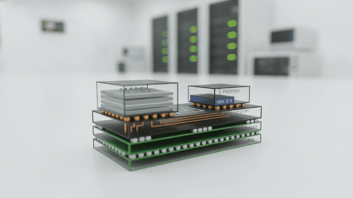
AMD & Qualcomm introduce Versal MoP & HBC, structurally solving memory bandwidth issues and reducing HBM dependency for AI & HPC.
The semiconductor industry is fundamentally re-architecting its approach to memory packaging, a structural response to the persistent data transfer bottlenecks that challenge modern computing. This shift is driven by the insatiable demands of artificial intelligence (AI) and high-performance computing (HPC) workloads, which increasingly push the limits of traditional memory architectures and their ability to feed data to processors at requisite speeds.
AMD and Qualcomm have notably contributed to this evolving landscape, each introducing distinct packaging innovations designed to circumvent the ‘memory wall’ – the critical impediment where processor speeds outpace memory access rates. These developments signal a broader industry trend towards integrated, specialized solutions to optimize performance, manage costs, and bolster supply chain resilience, offering alternatives amidst the current shortages and high costs associated with High Bandwidth Memory (HBM) and its complex packaging requirements.
The Fundamental Challenge: The Memory Wall
At its core, the memory wall represents a fundamental physics and economic challenge: moving data. Modern processors, particularly those designed for AI and parallel computing, can execute trillions of operations per second. However, their true potential remains constrained if data cannot be delivered from memory fast enough. This bottleneck is not merely about raw bandwidth, but also encompasses latency and the significant energy consumption associated with long data pathways between discrete components.
Traditional memory architectures, even advanced ones like HBM, face inherent limitations. While HBM offers substantial bandwidth improvements by stacking DRAM dies vertically and integrating them closely with the processor on an interposer, its adoption has been hampered by factors such as high manufacturing costs, intricate packaging processes, and, crucially, supply chain constraints that have led to shortages. This creates an economic incentive for alternative structural solutions that can deliver comparable or superior system-level performance characteristics without the same dependencies.
The Framework: Heterogeneous Integration as a Solution
The industry’s structural response to the memory wall and HBM’s limitations is increasingly centered on heterogeneous integration. This framework involves combining different types of chips—logic, memory, and specialized accelerators—within a single, tightly integrated package, often leveraging advanced 2.5D or 3D stacking technologies. The underlying principle is to minimize the physical distance data must travel, thereby reducing latency, increasing bandwidth, and improving power efficiency by drastically shortening interconnects compared to traditional board-level connections.
This paradigm shift moves beyond the conventional approach of discrete components on a printed circuit board (PCB). Instead, it embraces a system-in-package (SiP) philosophy, where multiple dies are co-located and interconnected with high-density, low-latency interfaces. This integration fundamentally alters the design calculus, allowing for optimized data flow and power delivery, which are critical for the demanding workloads of AI data centers and industrial applications.
Evidence of a Shifting Landscape: MoP and HBC
Concrete evidence of this structural shift is manifest in the recent introductions by AMD and Qualcomm. AMD’s Versal Premium Gen 2 Memory on Package (MoP) exemplifies a highly integrated solution designed for industrial applications. This technology directly integrates DRAM with a System-on-Chip (SoC) within the same package. The immediate benefits are substantial: high bandwidth capabilities are achieved through proximity, alongside significant board area savings. This approach simplifies system design for specialized industrial use cases where space and performance density are paramount.
Qualcomm’s High Bandwidth Compute (HBC) offers another compelling illustration, targeting AI data centers with a 2.5D-like technology. HBC combines an AI chip with stacked LPDDR DRAM, presenting a powerful alternative to existing solutions. Qualcomm reports that HBC delivers significant improvements in bandwidth and capacity per watt when compared to both HBM and SRAM. This focus on